There are many ways to make LTPS films on glass or plastic substrates:
TFT – LCD profile
What is TFT LCD?
TFT: Thin-film transistor
LCD: Liquid crystal display (LCD)
TFT-LCD was invented in 1960 and successfully commercialized as a notebook computer panel in 1991 after continuous improvement, thus entering the TFT-LCD generation.
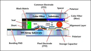
TFT – LCD structure:
Simply put, the basic structure of the TFT-LCD panel is a layer of liquid crystal sandwiched between two glass substrates. The front TFT display panel is coated with a color filter, and the back TFT display panel is coated with a thin film transistor (TFT). When a voltage is applied to the transistor, the liquid crystal turns and light passes through the liquid crystal to create a pixel on the front panel. The backlight module is responsible for providing the light source after the TFT-Array panel. Color filters give each pigment a specific color. The combination of each different color pixel gives you an image of the front of the panel.

TFT Pixel Element:
The TFT panel is composed of millions of TFT devices and ITO (In TI Oxide, a transparent conductive metal) regions arranged like a matrix, and the so-called Array refers to the region of millions of TFT devices arranged neatly, which is the panel display area. The figure below shows the structure of a TFT pixel.

No matter how the design of TFT display board changes or how the manufacturing process is simplified, its structure must have a TFT device and control liquid crystal region (if the light source is penetration-type LCD, the control liquid crystal region is ITO; but for reflective LCD, the metal with high reflection rate is used, such as Al).
The TFT device is a switch, whose function is to control the number of electrons flowing into the ITO region. When the number of electrons flowing into the ITO region reaches the desired value, the TFT device is turned off. At this time, the entire electrons are kept in the ITO region.

The figure above shows the time changes specified at each pixel point. G1 is continuously selected to be turned on by the driver IC from T1 to TN so that the source-driven IC charges TFT pixels on G1 in the order of D1, D2, and Dn. When TN +1, gATE-driven IC is selected G2 again, and source-driven IC is selected sequentially from D1.

The figure above can express several things:
The more vertical the Angle at which the LIQUID crystal stands, the more light will not be guided by the LIQUID crystal. Different liquid crystal standing angles will direct different amounts of light. From the above examples, the larger the angle at which the liquid crystal stands, the weaker the light that can be penetrated. (The direction of the upper and lower polarizer will determine the intensity of penetration, so as long as you understand the Angle of the liquid crystal standing will guide the intensity of light).
Undirected light is absorbed by the upper polarizer. Natural light is polarized in any direction. The function of the polarizer is to filter out most of the light oscillating in different directions and only allow light in a specific direction to pass through.
What is the relationship between glass substrate size and generation?
Many people don’t understand the differences between generations of TFT-LCD plants, but the principle is quite simple. The main difference between generations of plants is in the size of glass substrates, which are products cut from large glass substrates. Newer plants have larger glass substrates that can be cut to increase productivity and reduce costs, or to produce larger panels (such as TFT display LCD TV panels).
The TFT-LCD industry first emerged in Japan in the 1990s, when a process was designed and built in the country. The first-generation glass substrate is about 30 X 40 cm in size, about the size of a full-size magazine, and can be made into a 15-inch panel. By the time Acer Technology (which was later merged with Unioptronics to become AU Optronics) entered the industry in 1996, the technology had advanced to A 3.5 generation plant (G3.5) with glass substrate size of about 60 X 72 cm.Au Optronics has evolved to a sixth-generation factory (G6) process where the G6 glass substrate measures 150 X 185 cm, the size of a double bed. One G6 glass substrate can cut 30 15-inch panels, compared with the G3.5 which can cut 4 panels and G1 which can only cut one 15-inch panel, the production capacity of the sixth generation factory is enlarged, and the relative cost is reduced. In addition, the large size of the G6 glass substrate can be cut into large-sized panels, which can produce eight 32-inch LCD TV panels, increasing the diversity of panel applications. Therefore, the global TFT LCD manufacturers are all invested in the new generation of plant manufacturing technology.
Introduction to TFT-LCD manufacturing process
What is TFT LCD?
The TRANSISTor-LCD is an acronym for thin-film TFT Display. Simply put, TFT-LCD panels can be seen as two glass substrates sandwiched between a layer of liquid crystal. The upper glass substrate is connected to a Color Filter, while the lower glass has transistors embedded in it. When the electric field changes through the transistor, the liquid crystal molecules deflect, so as to change the polarization of the light, and the polarizing film is used to determine the light and shade state of the Pixel. In addition, the upper glass is fitted to the color filter, so that each Pixel contains three colors of red, blue and green, which make up the image on the panel.
Three main stages of the TFT LCD production process:
The first Array
– The Array process in the front segment is similar to the semiconductor process, except that thin-film transistors are made on glass rather than silicon wafers.
Midway through the Cell
– The middle Cell is based on the glass substrate of the front segment Array, which is combined with the glass substrate of the color filter, and liquid crystal (LC) is injected between the two glass substrates.
Module Assembly
-The rear module assembly process is the production operation of assembling the glass after the Cell process with other components such as backlight plate, circuit, frame, etc.
Latest technology development
Organic light-emitting display
Organic Light EmitTIng Display, or OLED, is a technology that has the following superior use characteristics.
Spontaneous light
Ultra-thin characteristics
High brightness
High luminous efficiency
High contrast
Microsecond reaction time
Ultra-wide Angle of view
Low power consumption
Can use a wide range of temperature
Flexible panel
Low-temperature polysilicon

The luminescence principle is tied to the vapor electroplating organic film between the transparent anode and the metal cathode. The electron and electric hole are injected, and the energy is converted into visible light by the composite between the organic film. And can match different organic materials, emit different colors of light, to achieve the requirements of the full-color display.
Active OLED
The organic light display can be divided into Passive Matrix (PMOLED) and Active Matrix (AMOLED) according to the driving mode. The so-called active driven OLED(AMOLED) can be visualized in the Thin Film Transistor (TFT) as a capacitor that stores signals to provide the ability to visualize the light in a grayscale.
Although the production cost and technical barriers of passive OLED are low, it is limited by the driving mode and the resolution cannot be improved. Therefore, the application product size is limited to about 5″, and the product will be limited to the market of low resolution and small size. For high precision and large picture, the active drive is mainly used. The so-called active drive is capacitive to store the signal, so when the scanning line is swept, the pixel can still maintain its original brightness. In the case of passive drive, only the pixels selected by the scan line are lit. Therefore, in an active-drive mode, OLED does not need to be driven to very high brightness, thus achieving better life performance and high resolution.OLED combined with TFT technology can realize active driving OLED, which can meet the current display market for the smoothness of screen playback, as well as higher and higher resolution requirements, fully display the above superior characteristics of OLED.
The technology to grow The TFT on the glass substrate can be amorphous Silicon (A-SI) manufacturing process and Low-Temperature Poly-Silicon (LTPS). The biggest difference between LTPS TFT and A-SI TFT is the difference between its electrical properties and the complicated manufacturing process. LTPS TFT has a higher carrier mobility rate, which means that TFT can provide more current, but its process is complicated.A-si TFT, on the other hand, although a-Si’s carrier movement rate is not as good as LTPS’s, it has a better competitive advantage in cost due to its simple and mature process.Au Optronics is the only company in the world that has successfully combined OLED with LTPS and A-SI TFT at the same time, making it a leader in active OLED technology.
Low-temperature polysilicon
What is LTPS?
Polysilicon is a silicon-based material about 0.1 to several um in size, composed of many silicon particles. In the semiconductor manufacturing industry, polysilicon should normally be treated by Low-Pressure Chemical Vapor Deposition. If the annealing process is higher than 900C, this method is known as SPC. Solid Phase Deposition. However, this method does not work in the flat display industry because the maximum temperature of the glass is only 650C. Therefore, LTPS technology is specifically applied to the manufacture of flat displays.

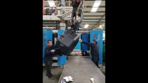
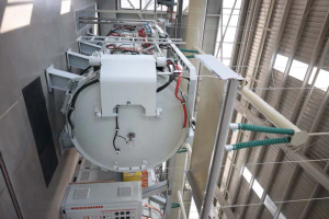
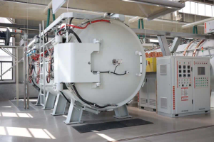
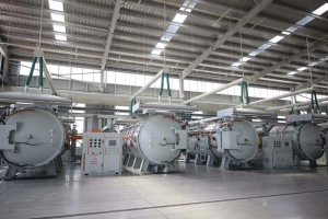
There are many ways to make LTPS films on glass or plastic substrates:
1. Metal partial action (MIC):
Let me suppose that it belongs to the SPC method. However, compared with traditional SPC, this method can produce polysilicon at low temperatures (about 500~600 C). This is because the thin layer of metal is coated before the formation of crystallization, and the metal composition plays an active role in reducing crystallization.
2. Cat-CVD:
A method for direct deposition of Poly-film without vapor extraction. The sedimentation temperature may be below 300C. Growth mechanisms contain catalytic cracking reactions of SiH4-H2 mixtures.
3. Laser Anneal:
This method is currently the most widely used. The Excimer laser is used for heating and melting A-SI. It contains low amounts of hydrogen and recrystallizes to Poly-film.
There are many ways to make LTPS films on glass or plastic substrates:
The LTPS membrane is much more complex than a-SI, yet the LTPS TFT is 100 times more mobile than A-SI TFT. And CMOS program can be carried out directly on a glass substrate. Here are some of the features that p-SI has over A-SI:
1. Thin-film transistors have faster mobility, so the drive circuit can be fabricated directly on the glass substrate, thus reducing the cost.
2. Vehicle for OLED: High mobility means that the OLED Device can provide a large driving current, so it is more suitable for an active OLED display substrate.
3. Compact module: As part of the drive circuit can be made on the glass substrate, the circuit on the PCB is relatively simple, thus saving the PCB area.
MVA
MVA technology not only improves the panel view but also solves most of the problems of gray-scale inversion due to the special arrangement mode of liquid crystals.
The advantages of using MVA technology include:
High contrast
Wide Angle of view
No grayscale inversion
High resolution
Quick response time

Half penetration and half reflection
LCD screens are backlit to project images through color filters before they are reflected in our eye Windows. This mode of carrying backlit LCD screens, known as “penetrating” LCD screens, consumes most of the power through backlit devices. The brighter the backlight, the brighter it will appear in front of the screen, but the more power it will consume.
The “reflective” architecture USES an external light source to display the image via a reflector, which saves electricity but is harder to see in the absence of an external light source.
“Half penetration and half reflection” is the compromise between the two. The device USES a half mirror instead of the reflector, which can not only pass through the backlight but also use the reflection from the external light source to achieve the effect of saving electricity, increasing brightness, and reducing weight.

COG
Different from the traditional manufacturing process, COG technology directly assumes the drive IC on the glass substrate. The advantages of this technology include:
Increased packing density and reduced weight make the panel thinner and lighter
Reduce the use of materials, reduce production costs
Improve panel resolution

ODF
ODF process is an epoch-making manufacturing method, which is time-consuming, low yield, and difficult to achieve in the past. Such as the production of large panels of TV products, in response to the rapid response of small Gap panels, or advanced high-quality MVA panels, using ODF process technology, the problem can be readily solved.
The simple comparison between traditional and ODF processes is as follows:

Using the ODF process, we can get the following advantages:
1. Decreased machine investment:
using the ODF process, we no longer need a vacuum tempering process, LIQUID crystal injection machine, sealing machine, and panel cleaning equipment after sealing.
2. Space and manpower savings:
As a result of the process reduction described in item 1, relative manpower and space savings were achieved.
3. Material saving:
Generally speaking, in the ODF process, the use efficiency of a LIQUID crystal is more than 95%, but compared with 60% of the traditional process, it can fully save more than 35% of the cost of liquid crystal materials. It can also save water, electricity, gas, and lotion when cleaning sealant and related panels.
4. Reduction of manufacturing time:
The manufacturing process saved is originally the most time-consuming and time-consuming process in the traditional manufacturing process. Moreover, with the trend of large-scale panels, or high-quality panels of small Cell Gap, the time will be longer. Traditionally, Cell processes take at least three days to complete, but ODF processes take less than one day.
Related posts:
The Viewing Angle of TFT LCD display Screens
How to set up the Raspberry PI Touch Screen
How TFT LCD Touch Screen Display Works
What are the Connection Methods of LCD liquid crystal screen
STONE Will Bring A Variety Of New Products To The 2018 India International Fair
Warm Congratulations on the Relocation of STONE Technology
Manufacturing purchasing managers’ index for July
The World’s Largest Production Base of Flexible Folding Screen Glass Substrate with A Total Investment of 6 Billion to Start Construction
About finding a new LCD display supplier. What do you need to know?
OLED/QLED/MicroLED: Next generation display Technology Who can challenge LCD?
.jpg "There are many ways to make LTPS films on glass or plastic substrates:")